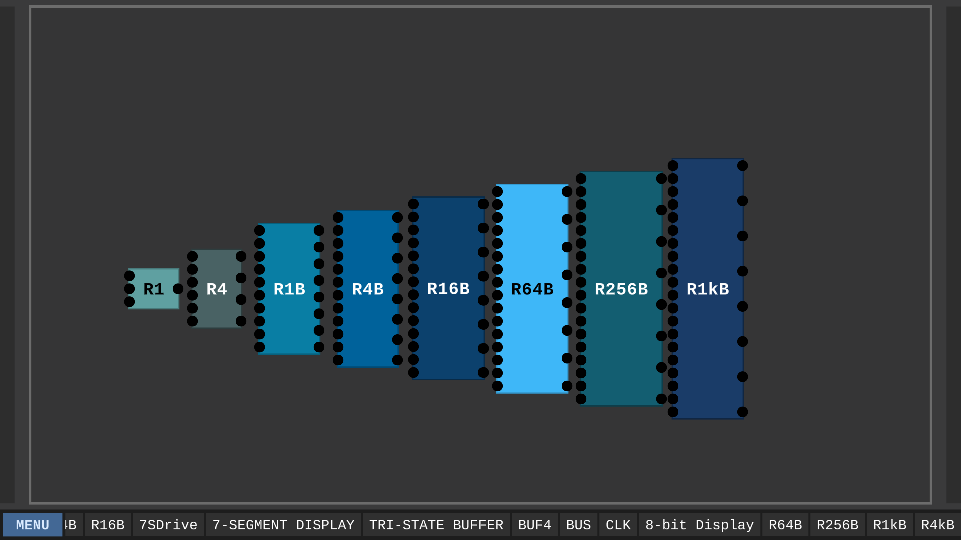
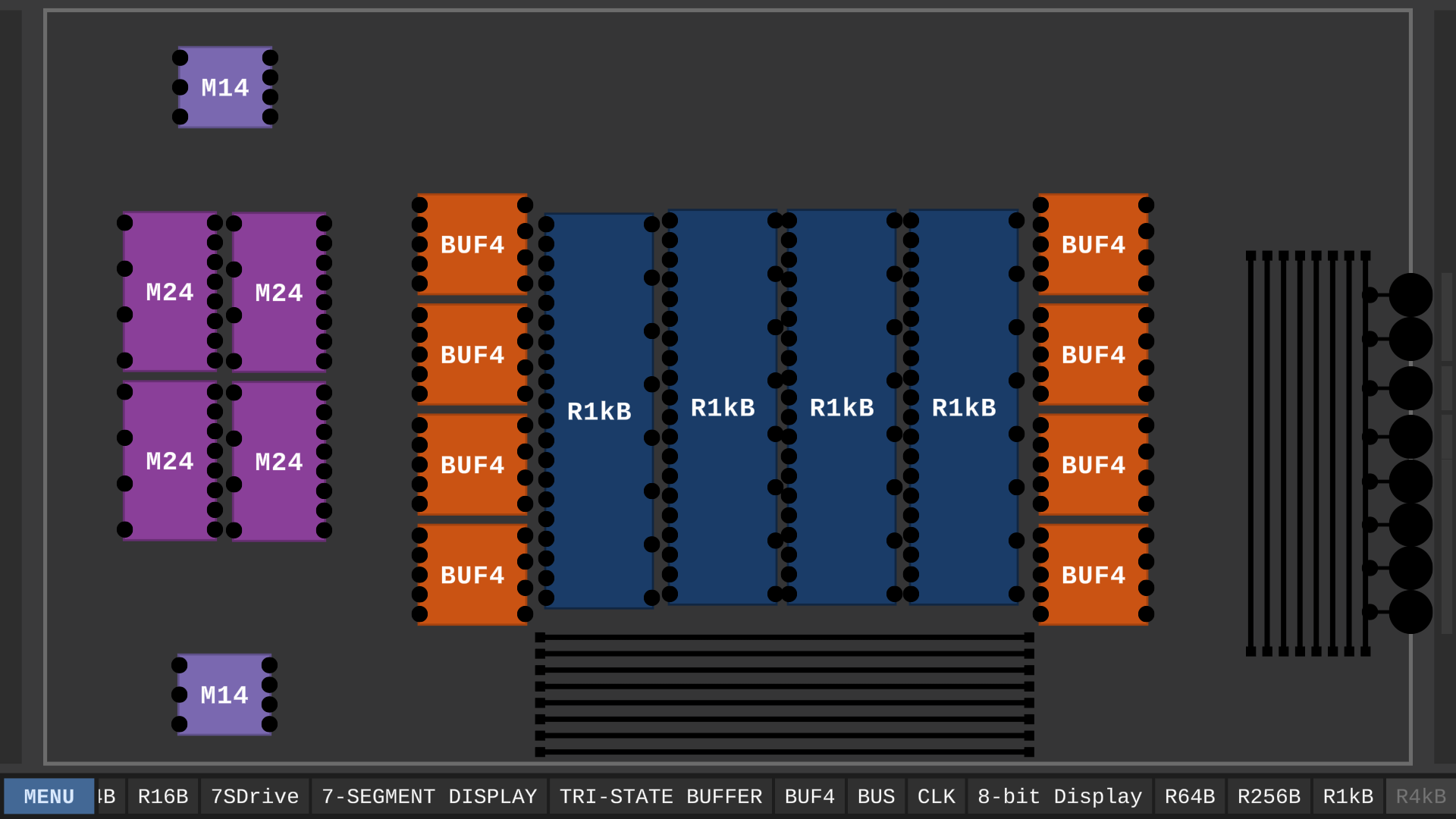
What I really wanted to do to try to impress this discussion board was figure out how to make a 1KB memory chip but I quickly realized it would either be utterly unfeasible or just take way too long.
A packaged chip, no. having 1KB of memory in the workspace? Maybe....... Probably not.
The next day.... I take it all back hold my bong.... (^^^Me being an idiot^^^)
The next NEXT day.... Alrighty, here's what I've come up with.... Man these colored wires and pins are a godsend!
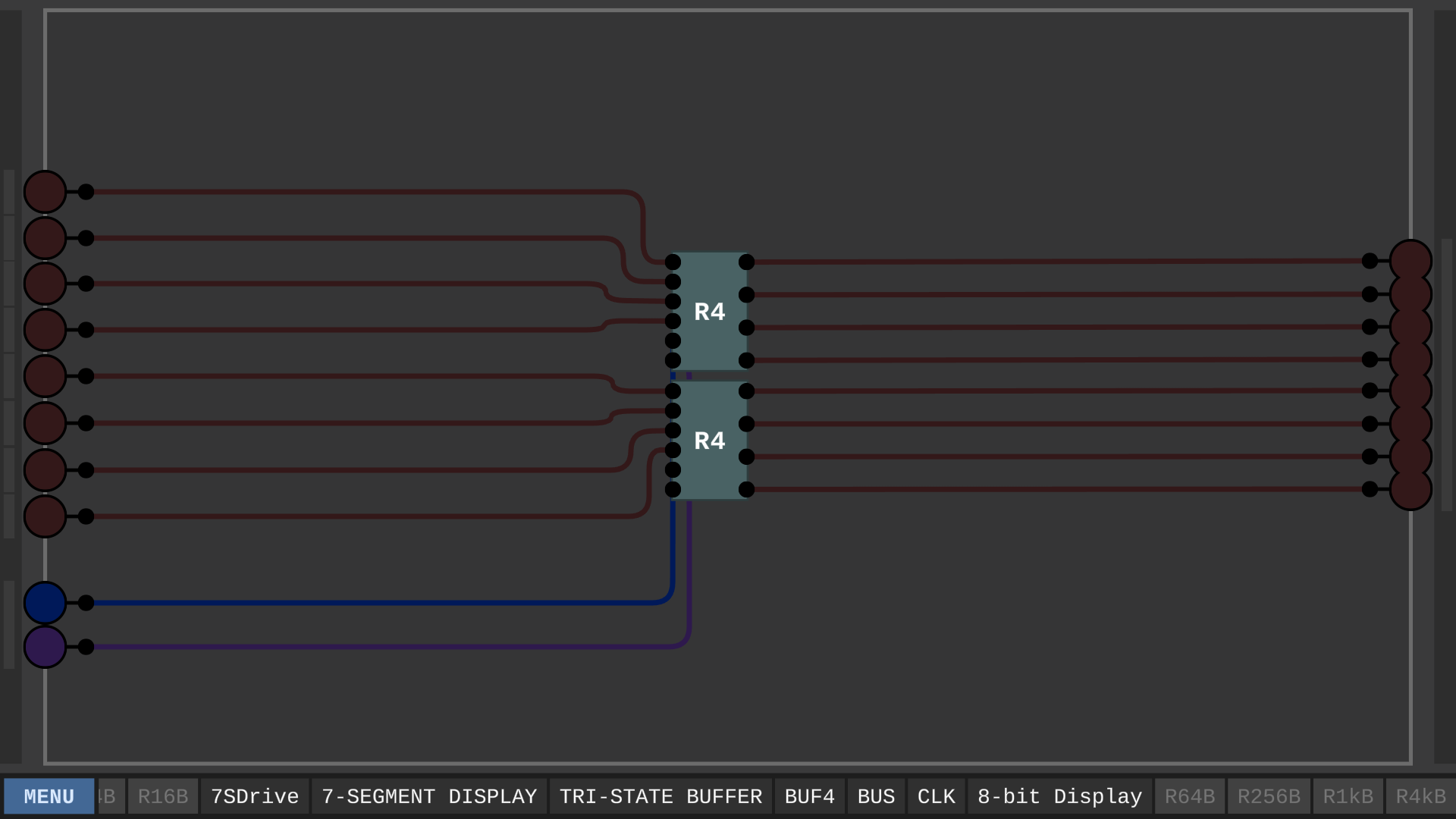
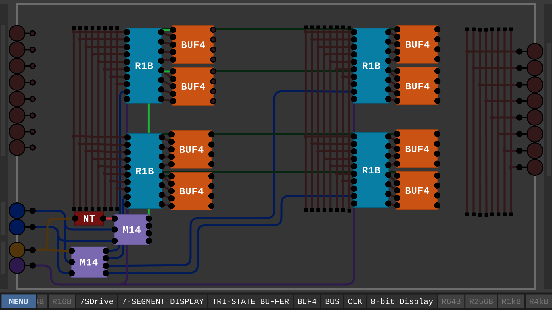
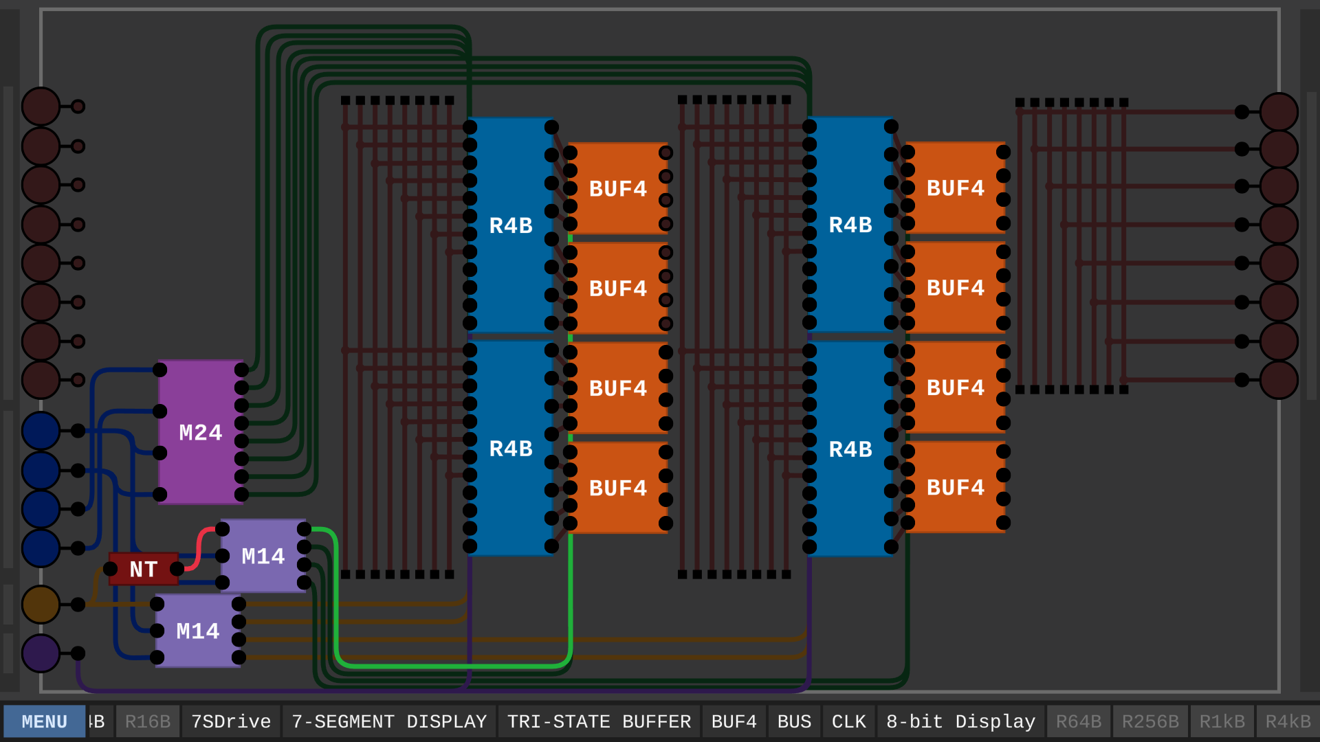
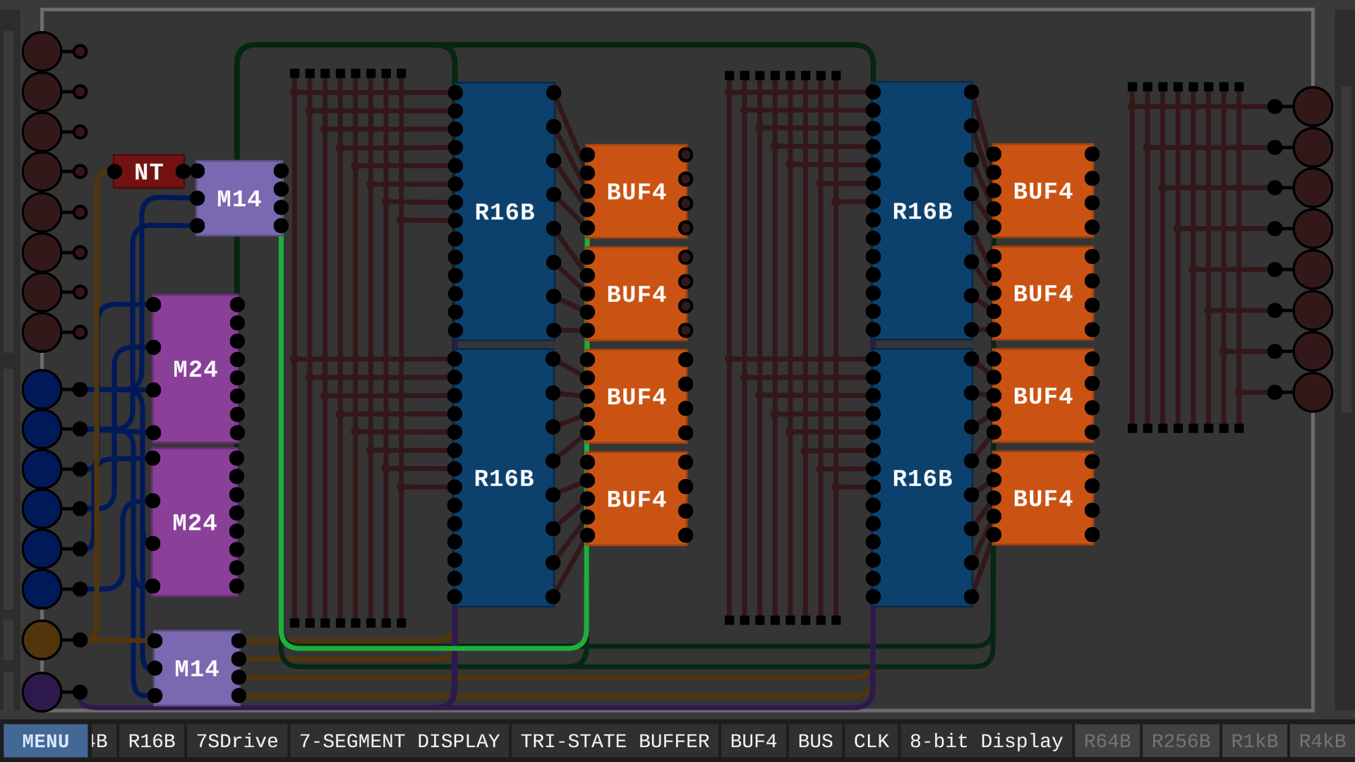
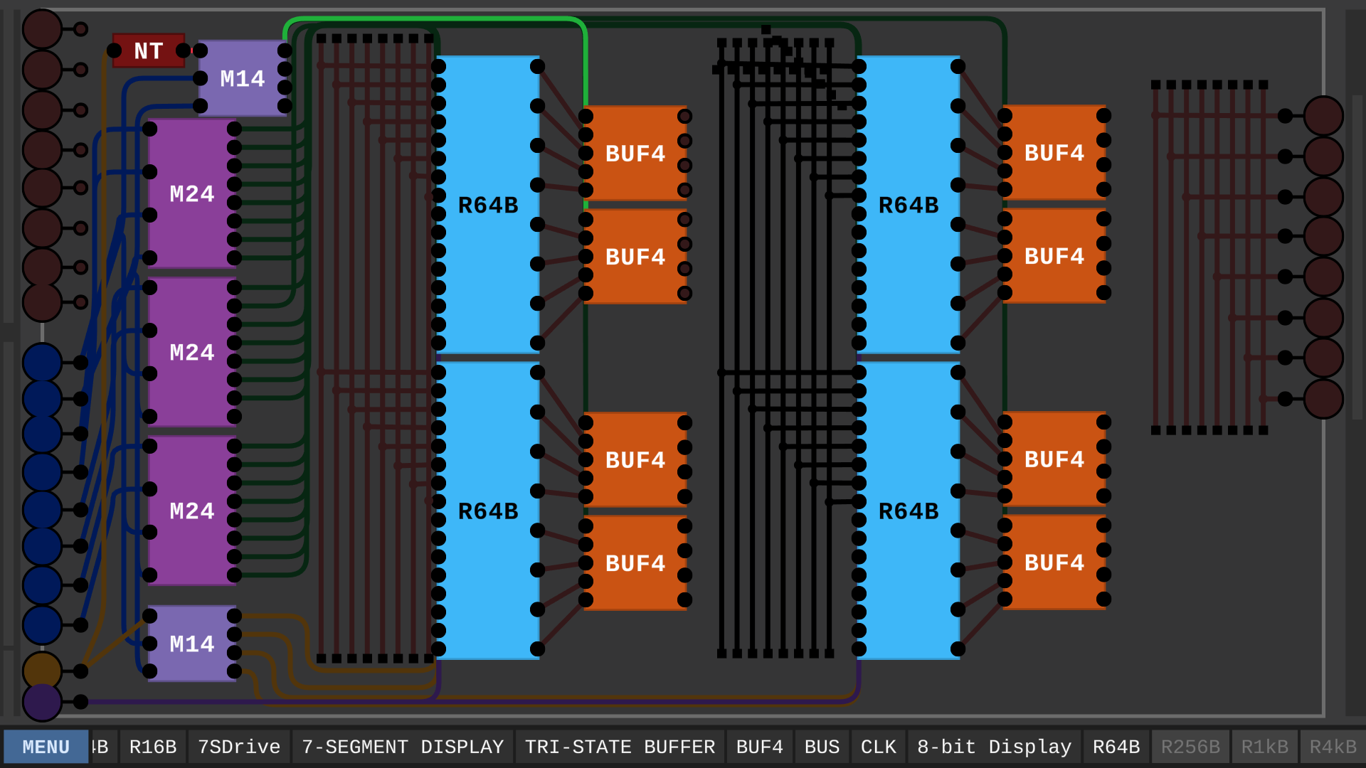
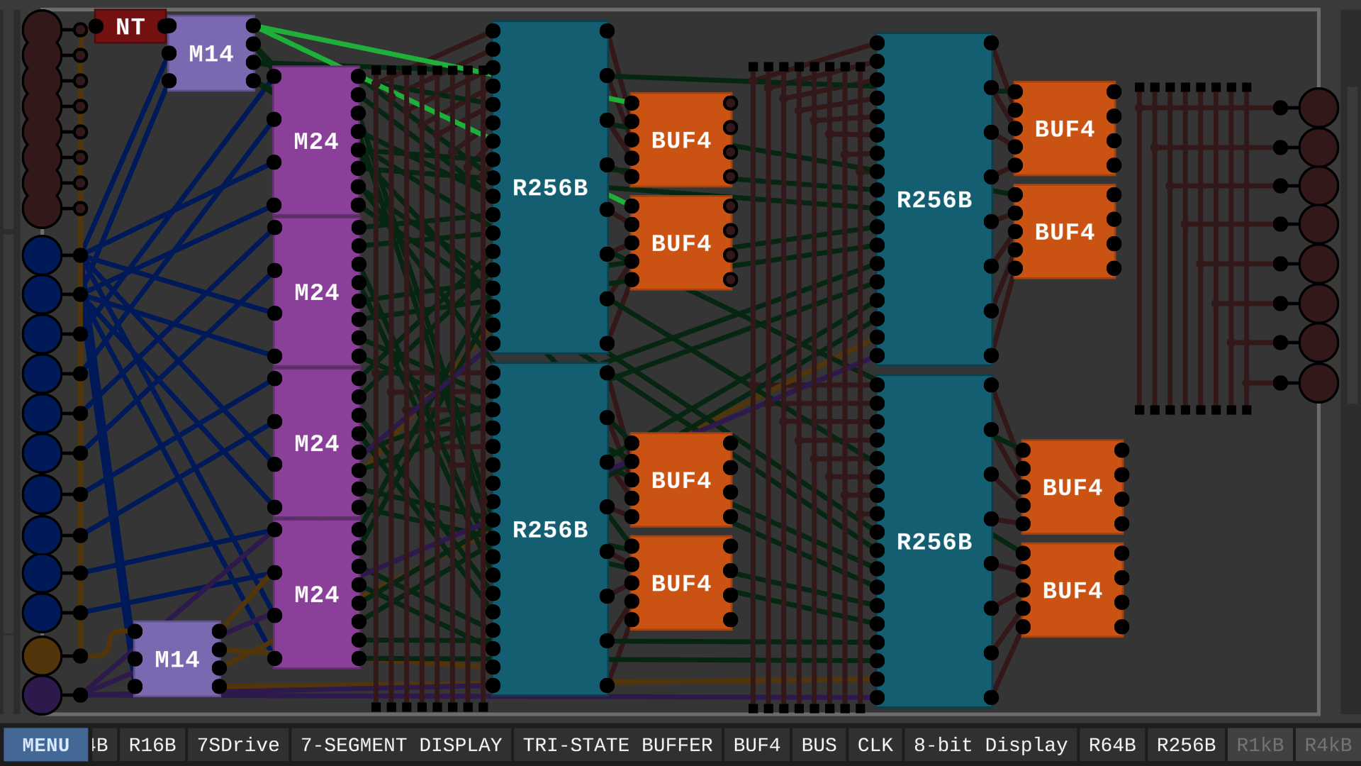
I've created a 4-byte memory chip in DLS that uses only 12 input pins and 8 output pins. Here's what it looks like!
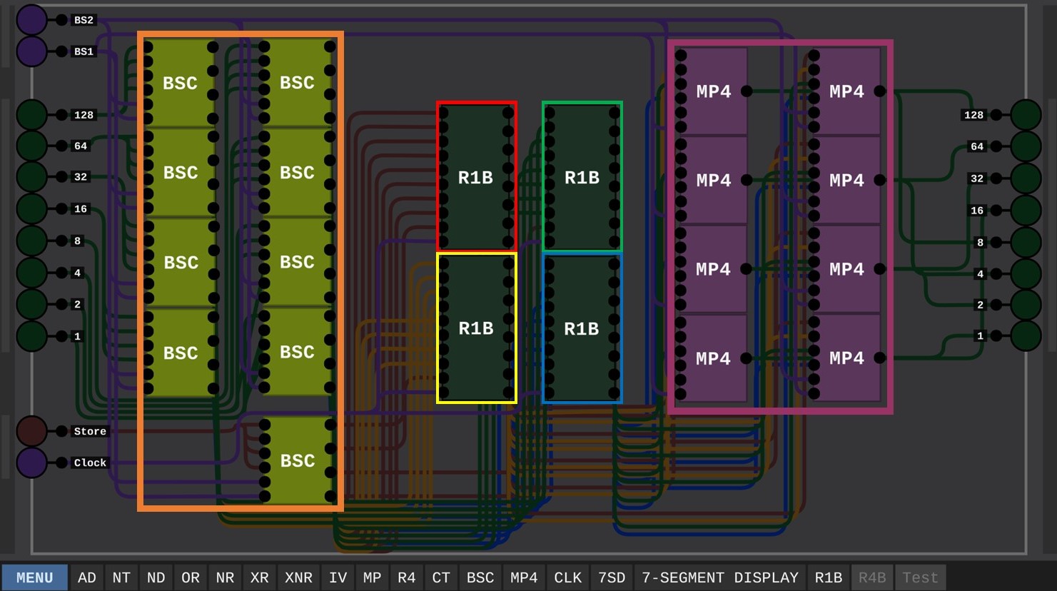
Let's get one thing out of the way first; Mainly in the interest of keeping the chips as small as possible, but also to have a basic notation that still let's me organize them, I have made my own shorthand names for these chips. Sorry if they're dumb!
Now, since that is the case, I should at least explain what each chip is;
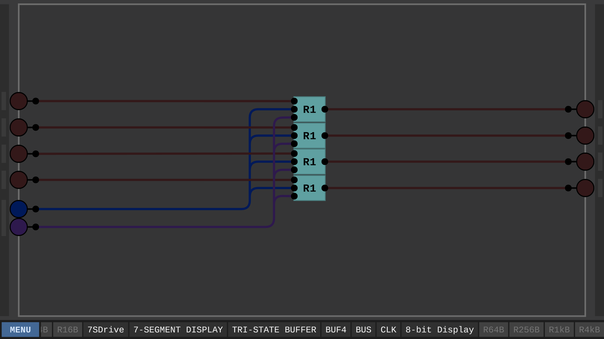
- [Orange] (*White and brown wires, please?) - It's a multiplexor with an additional bit-select pin, and 4 data-in pins, each paired with it's own data-out pin. They allow me to choose which 1-Byte register I want to send those 8 data-in bits to. There is one for each data-in bit.
- [RYGB] - These are 1-Byte registers. They've been outlined with the color of the wires they're connected to.
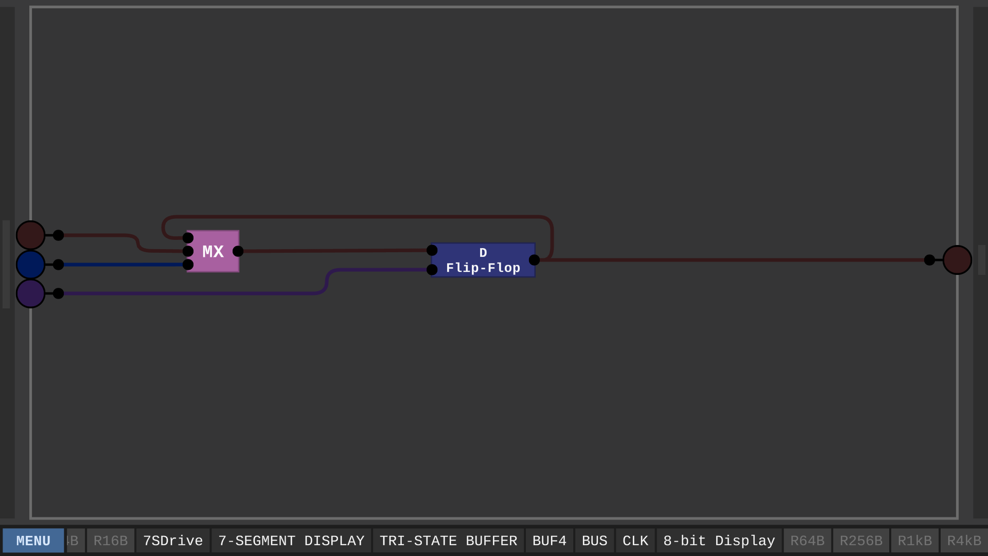
- [Magenta] - These are multiplexors with 4 inputs, all output on a single wire. There's one for each data-in signal, as well as the store signal.
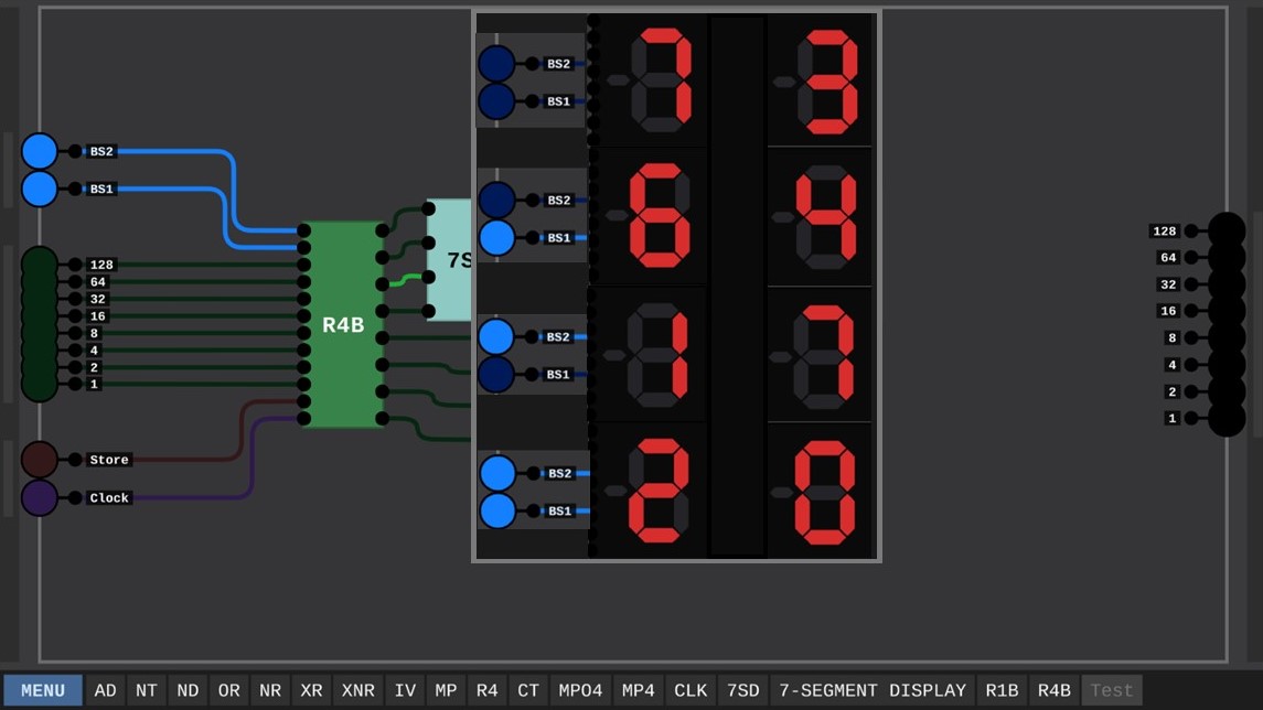
As you can see in the visualization above, The chip is quite small, not much bigger than the 1-byte registers within, and boy, it sure can store four 8-bit numbers! (8 BCD values in the example.)
So, why this design? Well, I'm hoping it's at least somewhat clever coming from someone who's quite inexperienced, since it seemed like the obvious path for me to take as far as keeping things parallel goes. Otherwise, moving data to-and-from the registers would become quite slow with the clock we have in the current version of DLS. (I do plan to make serial registers and share them here at some point, though, as it would drastically increase the storage I can squeeze out of DLS. 1kB would be a cakewalk..)
You may have noticed the two indigo, "BS1," and, "BS2," inputs in the corner. If I want to chain multiple of these registers together, they are going to be necessary. If I used a serial bus to direct data to these registers, they would be totally unnecessary, but even then it would be a good idea to keep them around I think.
With two bits, you can select 4 different bytes, and with just three, you can select 8 different bytes. Isn't that neat? With this design, for every doubling of the storage size, you only need one additional Byte-Select pin on the chip. In other words, the number of pins grows logarithmically with the number of Bytes. If I do build a 1kB memory chip, the number of input pins would be a mere 2% of the number of bytes the chip can store. [10 + log(#Bytes) = #pins] Isn't binary counting awesome?
Additionally, You don't necessarily need any more output pins than required to send 1 Byte of data. (1000 pins! |\{^o^}/|)
You might now be asking, "Well, Neutrino, just how big of a memory chip can you make with this method? Will you ever make it to 1kB?"
Uh, Good question! Wiring takes eons for my pea-brain to do. I'll let you know!
In any case, thanks for reading. Hope I did a good. :)
Cheers,
- Neutrino


