On Sale: GamesAssetsToolsTabletopComics
Indie game storeFree gamesFun gamesHorror games
Game developmentAssetsComics
SalesBundles
Jobs
TagsGame Engines

Going Serial

A topic by Neutrinos created Apr 20, 2023 Views: 854 Replies: 14
Viewing posts 1 to 9
(4 edits)

It's about time I started experimenting with serial encoding in DLS.

First things first, What's the difference between parallel and serial communication?
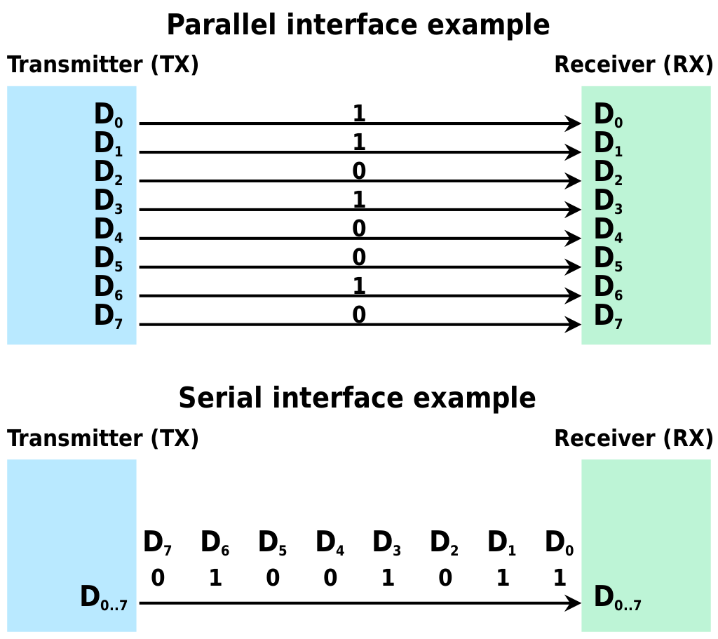


In Sebastian's amazing Digital Logic Sim YouTube series, all communication has been done in parallel. This is where we send a given amount of bits all at the same time on their own wires. For serial communication, we need to send those bits one after the other, over time, on a single wire.

We'll need two chips to do this. A serializer, and a deserializer.

The serializer will take in a parallel binary input, and convert it into a series of pulses that represent the original number.

The deserializer will take in that series of pulses and convert it back into the original number.

So, in reality, at least for the way I went about this, the serial output will require two wires. one for the clock signal, and one for the data signal.


Here's how that would look;
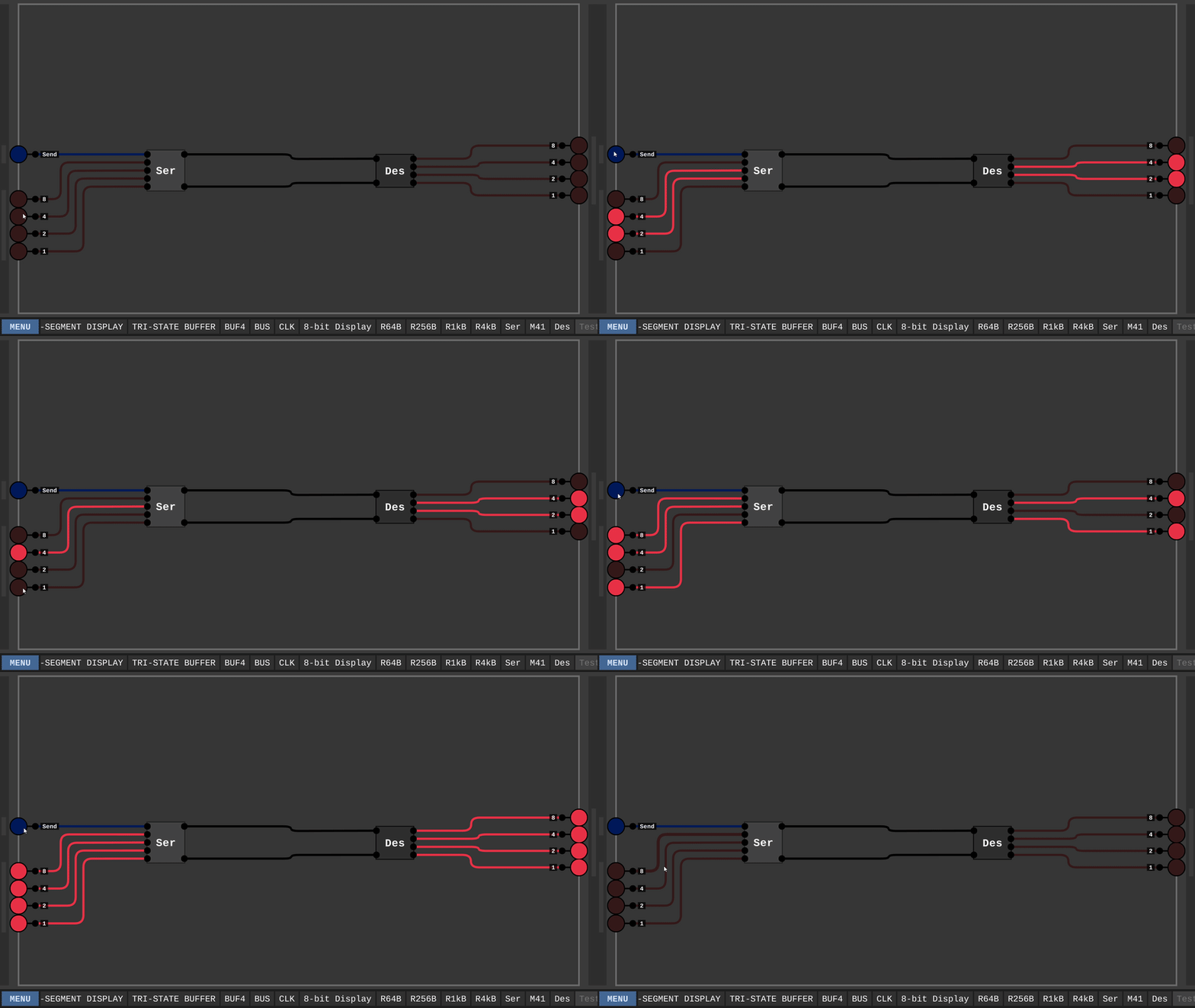

Pretty neat, right? Don't worry, it get's very ugly from here! Boy, I really need to rework these things to be simpler, or at least look nicer.

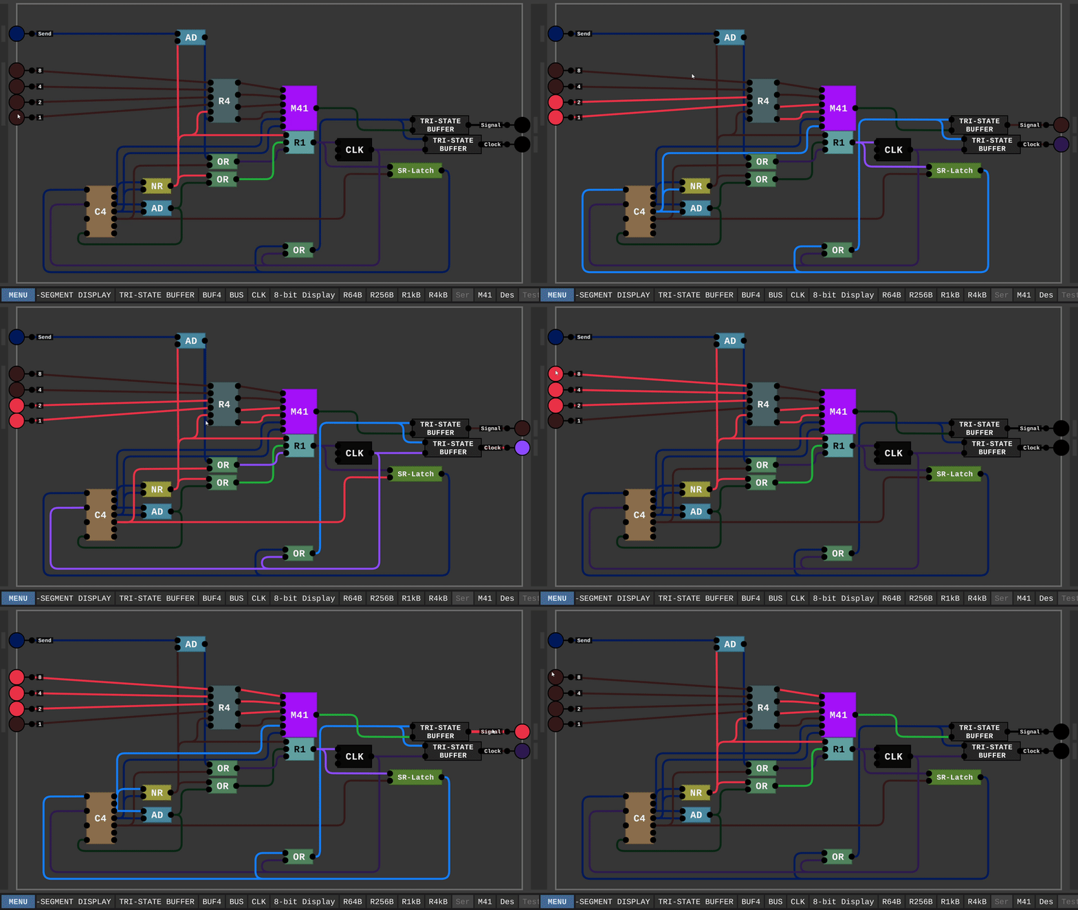
Alas, here are my first iterations of the serializer and deserializer;

Serializer:


Deserializer:
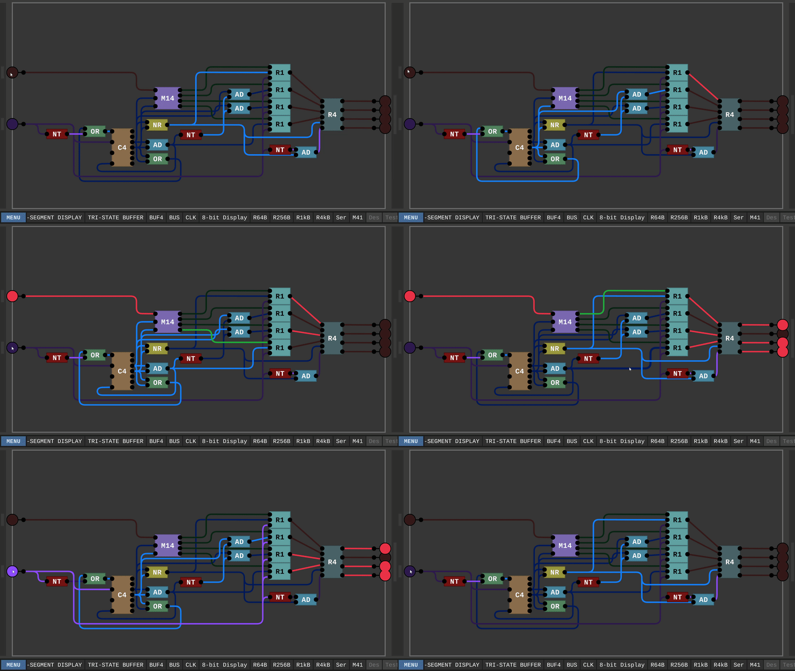

To be honest with you, I'm quite terrified to try and explain how these actually work. I'm almost certain there's a far better way to accomplish this behavior, but this is what I came up with.

Long story short, they both use a counter and multiplexor to select which bit is being written/read to/from a register. There is some logic to decide when the clock runs the counter, and some logic to decide when to write to the registers.

One concern for the future that I have, is that I've made the serializer with an internal clock. This may, or may not come back to haunt me later on.

And that's as much as I currently feel comfortable saying about these things! 

I'll happily answer any questions you ask to the best of my ability!

This one took some time to get right, as I pretty much just built it from scratch using the diagram I showed as my guide. I'd love to hear your opinions on it! I'd also love to see someone come up with their own version and share it with me. I can't wait to experiment with creating more components that use serialized signals!

That's all for now! I've more DLS hijinks to get up to! Thanks for reading! <3

(1 edit)

I'd also like to show my modified clock, since it's kinda the heart of the serializer;


The base clock runs constantly. The enable signal gets written to the register on the next rising edge of the clock. The register output is AND-ed with the base clock output. This ensures the clock always has a consistent output when being enabled, as the enable signal can't make the output pulse prematurely.

The F0 and F1 signals control the frequency of the clock.

Wow this is really cool! Good job 👍

Thank you! :)

What is the c4 and the M41 chips? Also if you go to %appdata% and then local low then sebastianLague and then V1 > Projects > (your save file) > then chips you can send the chip files for the serializer.

(1 edit)

Hey! Thanks for your response.

Sorry about the confusing short-handed chip names!

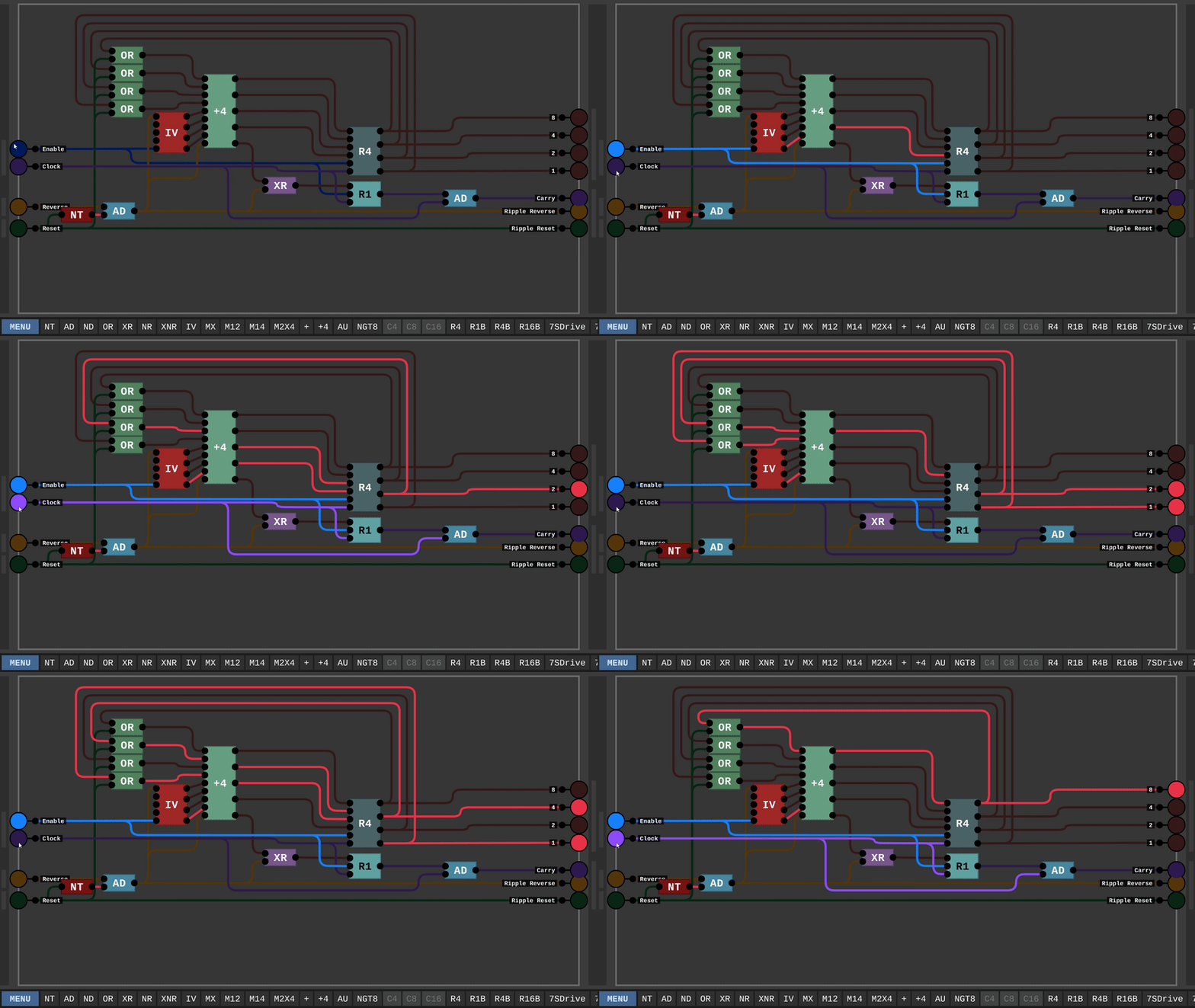
The "C4" Chip is a 4-bit counter I made.


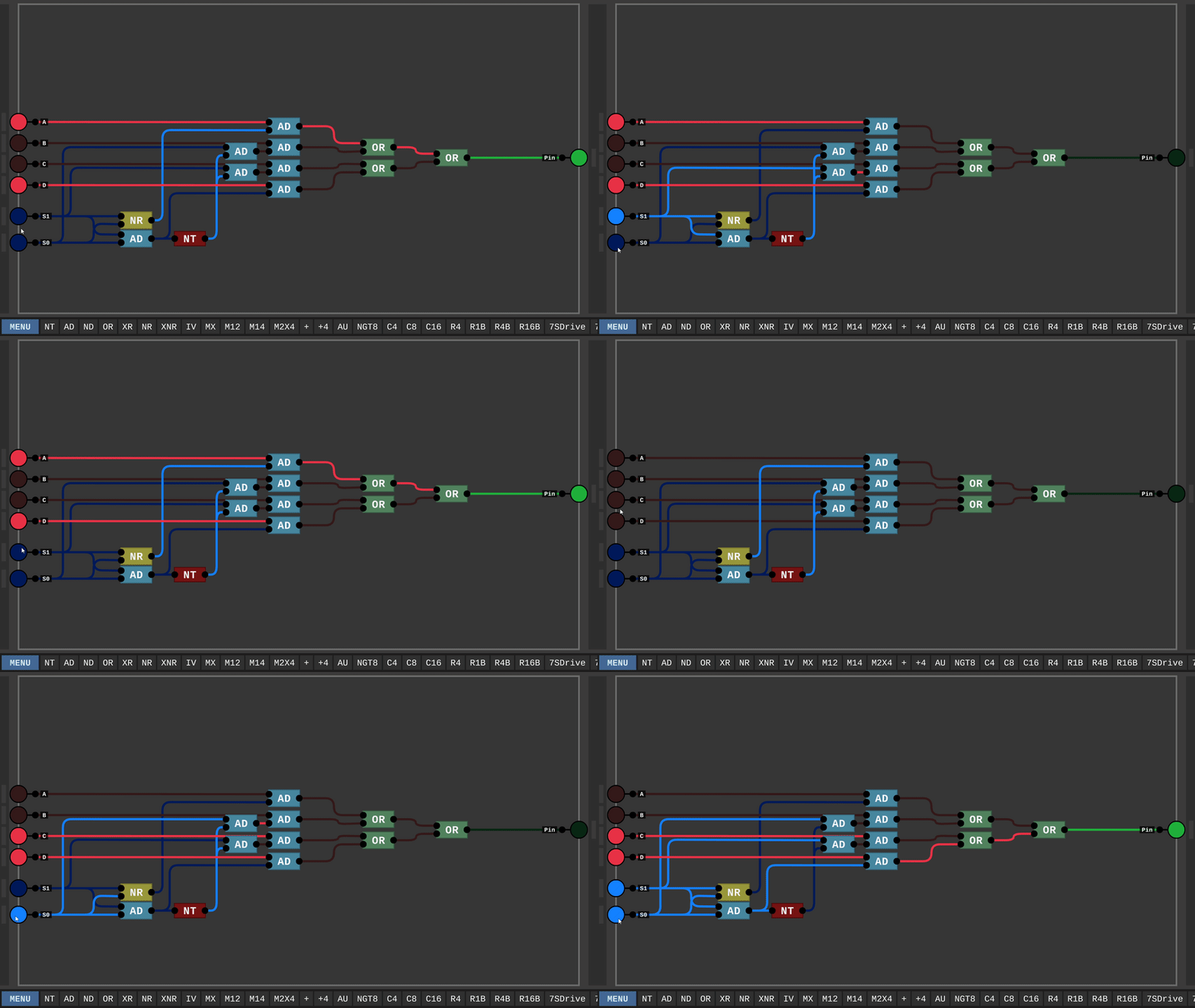
The "M41" Chip is a Multiplexer that chooses from four inputs to be sent to one output.


 As for sending my save, that's good to know! I'll attach the project file in this response after I give it a once-over. That way you can see how each chip was built!

Sorry but what's the IV chip. It appears to only effect the reverse so for now i do not necessary need it.

It's just a 4-bit inverter made with some XORs. 

When the reverse signal is turned on, it changes the 1 to a -1 so the counter can count backwards.

and the de multiplexor

If you mean the "M14" chip, it's practically the same as the "M41" chip, just backwards.


Keep the same selection logic, and hook one input up to all the AND gates. Ditch the OR gates and send the output of each AND gate to 1 of 4 outputs.

By the way, in your custom clock if you just turn up the speed of the original clock you can greatly improve the speed of your serializer.

(+1)

the custom click has pins for controlling the clock frequency :) super helpful if I need to slow it down to step through the logic.

Coming back to this I remember hand making the chips and now i switched computers and i cannot find them. Wonder if you still have them

(2 edits)

Hey, glad to know this hasn't been forgotten about after so long!

I do still have them, and I can attach the files if you like! To be honest though, I highly encourage attempting to make your own. Mine are, let's be honest, quite crude, and I'm sure you could come up with something better!

For now, here is the project file. I haven't done much with it since my last post, but I hope you enjoy it!

P.S. be careful of the large memory chips, they will lag DLS worse than Blighttown.

https://drive.google.com/drive/folders/1izAIND0fSJdlHVHxr_yGPsGMboNPWQWl?usp=dri...

could you show a picture of the IV chip? that would help me alot